New study shows that standard theoretical models accurately predict thermal behaviour in ordered nano-domains but fail in completely disordered materials because of randomised phonon scattering.



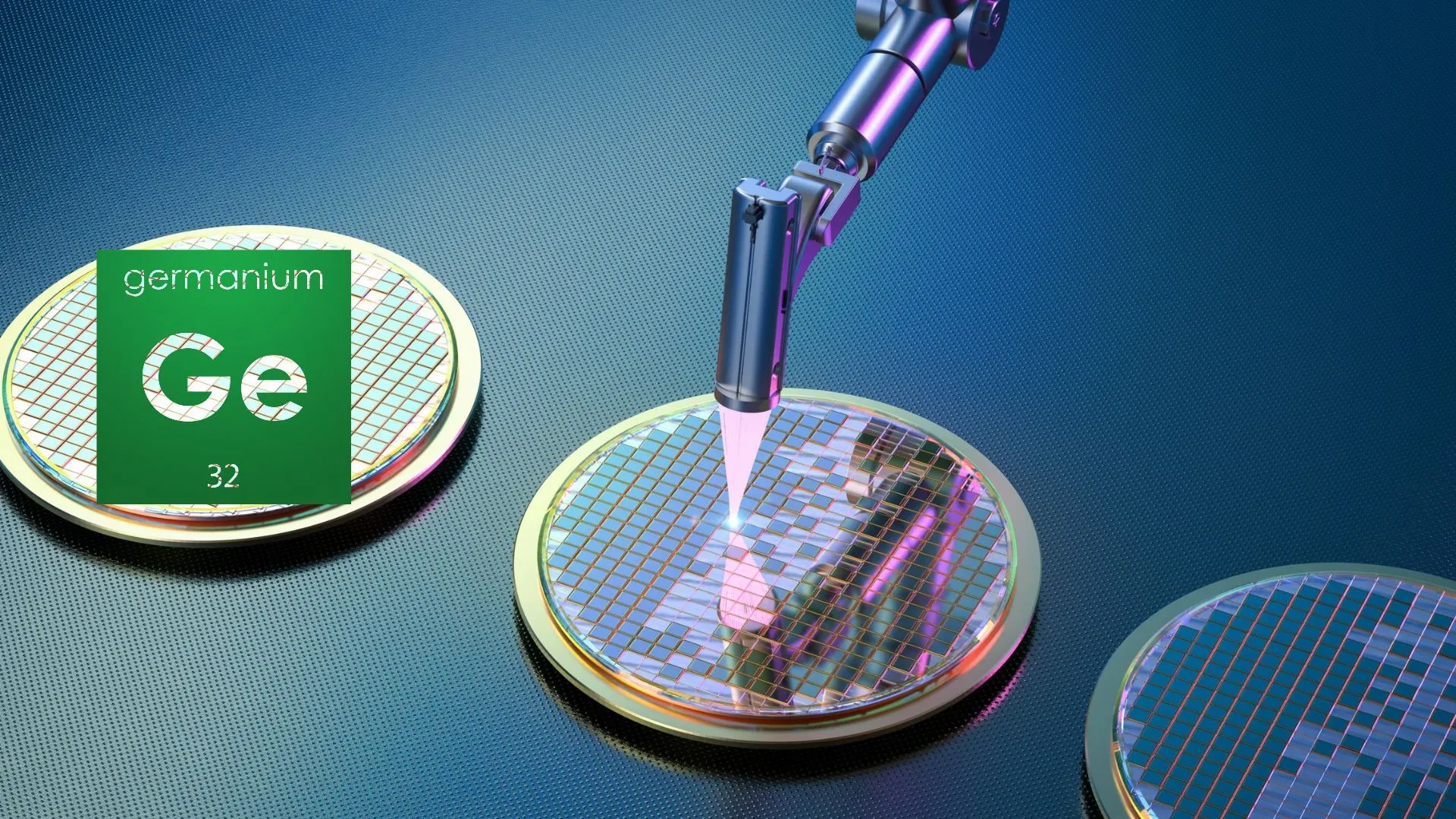
Germanium (Ge) is a greyish-white element with atomic number 32 and an indispensable part of modern electronic infrastructure, used in semiconductors, integrated circuits, LEDs, and solar cells. Researchers at the Indian Institute of Technology (IIT) Indore and the Raja Ramanna Centre for Advanced Technology (RRCAT) have investigated how microscopically thin Ge films respond to heat and laser energy. Their new study explores the thermal dynamics of low-dimensional germanium thin films, shedding light on how these materials behave under external thermal stimuli.
The team used Raman spectro-microscopy, which combines a high-resolution optical microscope with a Raman spectroscopy system to analyse the chemical composition of an element down to sub-micrometre resolution. They used this method to study both amorphous and nanocrystalline germanium thin films. Their study provides a clearer picture of how atomic arrangement dictates heat management in semiconductor components, which is critical for the ongoing evolution of multifunctional electronics, optoelectronic systems, and photonics.
The study focuses on phonons. Like photons, which are packets of light waves, phonons are quasiparticles that represent packets, or quantised units, of vibrational or acoustic energy in a crystal lattice. These lattice vibrations dictate how heat and energy move through a solid material. When a semiconductor is heated or exposed to laser light, its atomic lattice vibrates more intensely. This shifts its Raman scattering peaks to lower frequencies, a phenomenon known as phonon softening, and broadens them as phonon lifetimes shorten. By observing germanium films across a temperature range spanning up to 700 Kelvin, the researchers mapped these vibrational changes across both disordered amorphous phases and laser-annealed nanocrystalline phases.
To interpret their findings, the researchers used Balkanski’s well-known theoretical model, which mathematically accounts for how materials expand and change when heated. This formula examines how phonons break into smaller vibrations as temperatures rise. When they tested this formula on organised nanocrystalline germanium, the experimental results aligned closely with the model. Because these crystals have a neat, orderly structure, their vibrations follow predictable physics rules. As the material gets hotter, the vibrations break down in a steady, expected way, allowing scientists to track frequency shifts and line-width broadenings of a Raman spectrometer with high mathematical precision.
However, the team discovered a disagreement with theory when examining the amorphous germanium phase. Because this material lacks an orderly grid pattern, its atomic vibrations scatter in completely random, chaotic ways. Consequently, while amorphous germanium still undergoes peak softening due to thermal expansion, its spectral line-width changes show a chaotic, randomised pattern that standard anharmonic models or vibrational density of states alone cannot explain.
This research moves beyond bulk material assumptions and directly compares how different structural phases of the same semiconductor manage thermal energy side by side. Past investigations often treated low-dimensional systems with generalised models or struggled to isolate the exact transition thresholds between amorphous and crystalline states. By employing localised laser annealing paired with high-resolution thermal Raman mapping, the researchers successfully captured the exact transitional zone where partial crystallisation occurs. This method shows that laser exposure permanently alters the material from a disordered matrix into organised dendritic nanocrystals averaging about 6.6 nanometers.
As electronic devices continue to shrink toward the nanoscale, understanding these microscopic thermal responses will matter. As computer chips, microprocessors, and optoelectronic sensors pack more power into smaller footprints, managing heat dissipation becomes one of engineering’s greatest hurdles. By mapping how heat travels, scatters, and decays differently across amorphous and nanocrystalline semiconductor architectures, this research provides the foundational framework required to design smarter, thermally resilient electronic materials that can withstand intense operational stress without degrading.